美国操逼网,这里有精品久久,大屁屁少妇p,日本 欧美 一区 二区
<style id="b2rkw"></style>
<bdo id="b2rkw"><span id="b2rkw"><meter id="b2rkw"></meter></span></bdo>
<center id="b2rkw"><optgroup id="b2rkw"></optgroup></center>
<p id="b2rkw"></p>
<sub id="z2zom"><label id="z2zom"><label id="z2zom"></label></label></sub>
<bdo id="z2zom"><pre id="z2zom"><del id="z2zom"></del></pre></bdo>
Home
Product Center
SRAM
Low Power SRAM
Serial RAM
Async Fast SRAM
pSRAM
XRAM
NV RAM
MRAM
STT-MRAM
FeRAM
NV-SRAM
SDRAM
DRAM
SDR SDRAM
DDR1 SDRAM
DDR2 SDRAM
DDR3/4 SDRAM
Microcontroller
32bit MCU
8bit MCU
RISC-V MCU
DualCoreMCU
Product Solutions
Flash
MCP
Nand Flash
EEPROM
SPI NAND Flash
SPI Nor Flash
Bluetooth
Macrogiga
BLE 5.0
Voice recognition
solution
BLE Application
SOC Chip
PMICs
Dialog
Li-ion protection chip
CPLD
Discrete devices
SIC MOSFET
SIC SBD
Op Amp
Analog chip
ADC
AFE
Motor Driver
High Side Drive
Sensor
Other
Interface chip
Bare Die/Wafer
Switch
Memory
Support
Case Studies
Customer Service
News
News & Events
Notice
Industry News
About Us
Company profile
Organization
Contact Us
Contact Us
EN
CN
Notice
Everspin xSPI STT-MRAM code and data integration application scenario
Everspin's MRAM
NetSol Co., Ltd
Everspin’s NVMe Storage Accelerator mixes MRAM, UltraScale FPGA, delivers 1.5M
Home ?
Product Center
?
Other
?
Bare Die/Wafer
?
LM5025A Die
?
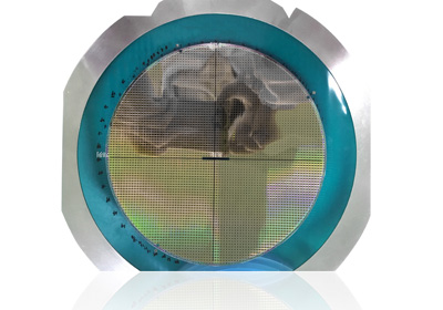
A wafer, also called a slice or substrate, is a thin slice of semiconductor material, such as a crystalline silicon, used in electronics for the fabrication of integrated circuits and in photovoltaics for conventional, wafer-based solar cells. The wafer serves as the substrate for microelectronic devices built in and over the wafer and undergoes many microfabrication process steps such as doping or ion implantation, etching, deposition of various materials, and photolithographic patterning. Finally the individual microcircuits are separated (dicing) and packaged.
Bare Die
MRAM
Low Power SRAM
Fast SRAM
LM5025A Die
LM5025A Die
Active Clamp Voltage Mode PWM Controller
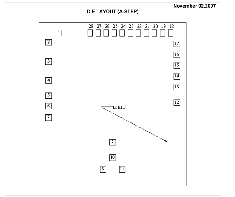
DIE/WAFER CHARACTERISTICS
Fabrication Attributes
General Die Information
Physical Die
Identification
LM5025A
Bond Pad Opening Size (min)
91μm x 91μm
Die Step
A
Bond Pad Metalization
Al_ 0.5%Cu
Physical Attributes
Passivation
PECVDOX+NITRIDE
Wafer Diameter
150mm
Back Side Metal
BARE BACK
Die Size (Drawn)
2286μm x 2540μm 90.0mils x 100.0mils
Back Side Connection
Floating
Thickness
254μm Nominal
Min Pitch
167μm Nominal
Special Assembly Requirements:
Note: Actual die size is rounded to the nearest micron.
LM5025 MDC MWC
ACTIVE CLAMP VOLTAGE MODE PWM CONTROLLER
Product Center
SRAM
NV RAM
SDRAM
More+
Support
Case Studies
Customer Service
News
News & Events
Notice
Industry News
About Us
Company profile
Organization
Contact Us
Contact Us
Service hotline:
+86-755-66658299
Buying online
The ? 2016 Shenzhen Ramsun Micro-electronincs Co., Ltd.|HK Ramsun International Limited
Guangdong ICP for 16037113
Open
Close
2647314998
2281572285
ramsun02
Tel
+86-13751192923
Use of cookies
We use cookies and similar technologies (also from third parties) to collect your deviceand browser information for a better understanding on how you use our online offerings.This enables us to optimize and personalize your experience with Ramsun and to provideyou with additional services and information based on your individual profile. Details areavailable in our privacy policy where you can also change your preferences on cookies atany time.
Reject
Accept